
A process-based technical article for PCB manufacturers.
This article summarizes an on-site production evaluation of Taiyada HC-1538B dry film photoresist. It focuses on what should be checked when visually darker and lighter material is observed during PCB imaging.
Key conclusion: visible film color variation should be assessed through controlled production results, not appearance alone.
1. What Was Observed
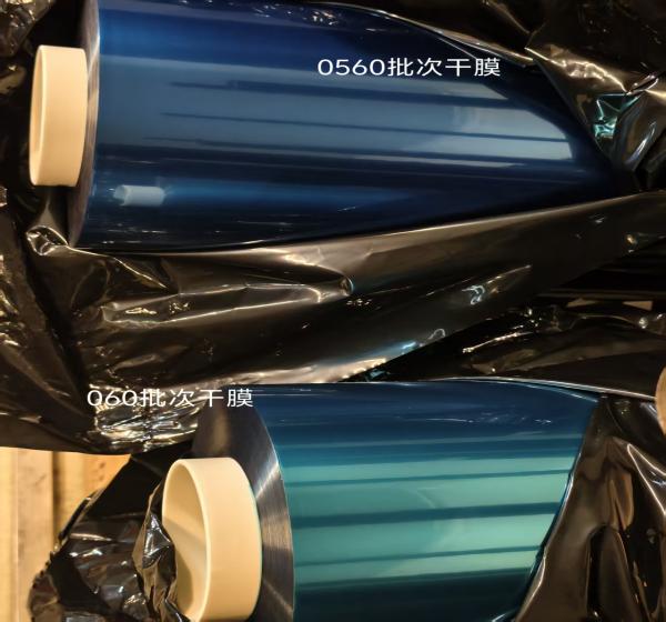
During production, different HC-1538B dry film rolls showed visible color variation. Some material appeared darker and some lighter. The engineering question was whether this visual difference would affect exposure, development, or final PCB quality.
The material was evaluated through the complete imaging flow: incoming material, surface preparation, lamination, LDI exposure, development, pattern plating, etching, and AOI inspection. This matters because a defect found after imaging may originate in a later process rather than in the dry film itself.
2. Process Conditions Used for the Evaluation
The recorded production conditions provide context for the evaluation. They are process references from this case, not universal settings for every PCB line.
Surface Preparation
| Parameter | Actual Condition | Recommended Condition | Reference Range |
|---|---|---|---|
| Line speed | 2.5–3.5 m/min | 3.0 m/min | 2.5–3.5 m/min |
| Drying temperature | 90°C | 90°C | 80–95°C |
| Washing pressure | 1.5 kg/cm² | 1.5 kg/cm² | 1.2–2.0 kg/cm² |
| Acid concentration | 4.5% | 4.5% | 3–5% |
Lamination
| Parameter | Actual Condition | Recommended Condition | Reference Range |
|---|---|---|---|
| Lamination speed | 1.8–2.0 m/min | 1.5 m/min | 1.8–2.0 m/min |
| Upper / lower roll temperature | 110°C / 110°C | 110°C / 110°C | 110–120°C |
| Board exit temperature | 45°C | 50°C | 45–65°C |
| Air pressure | 4.5 kg/cm² | 4.5 kg/cm² | 3.8–5.0 kg/cm² |
3. Exposure Energy Must Be Verified
The report records LDI exposure-energy control at 280–300 mA, with an exposure-scale control reference of approximately 6–7 steps. The operational recommendation was to confirm exposure energy about every four hours when processing material with different apparent color characteristics.
An exposure scale and actual imaging result are more reliable than judging exposure condition by film color alone. This helps prevent exposure drift from being mistaken for a material issue.
4. Darker Material May Show a Slower Post Exposure Image
For the darker portion of the evaluated material, the image appeared more slowly immediately after exposure. The recorded recommendation was to allow about 15–30 minutes, or longer when appropriate, before development and then assess the image result.
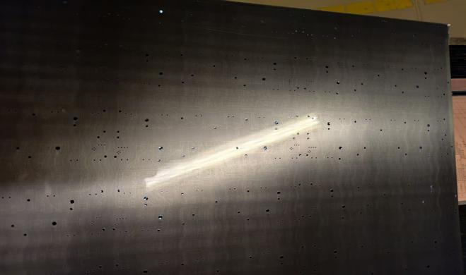
Operators should avoid changing production settings too quickly based only on immediate visual appearance. A suitable post-exposure holding time can prevent an unnecessary adjustment from introducing another process variable.
5. Development Conditions Must Be Checked Together
Exposure cannot be evaluated in isolation. Development point, spray pressure, developer concentration, and temperature should be verified at the same time.
| Developing Parameter | Actual Condition | Reference Range |
|---|---|---|
| Developing speed | 2.8–3.2 m/min | 2.8–3.2 m/min |
| Developing point | Upper about 40%; lower about 50% | 40–60% |
| Upper spray pressure | 1.2 kg/cm² | 1.2–1.5 kg/cm² |
| Lower spray pressure | 1.5 kg/cm² | 1.5 kg/cm² |
| Developer concentration | 1.0% | 0.8–1.2% |
| Developing temperature | 30°C | 28–32°C |
A practical troubleshooting approach is to evaluate exposure energy, developing point, and developing chemistry as one connected system. Adjusting only one parameter without confirming the others can make the cause of a problem harder to identify.
6. AOI Defects Require Root Cause Analysis
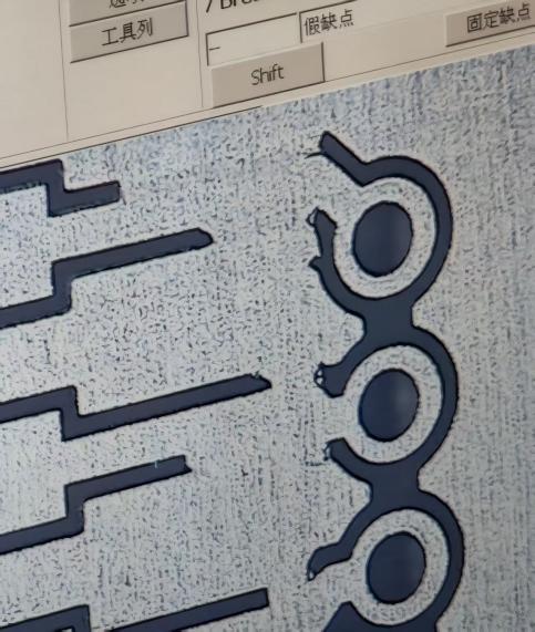
AOI inspection identified several defects that required further investigation. The report found that some copper-residue and short-circuit defects were associated with contamination or copper-wire carryover in the pattern-plating process. The recommended action was to maintain and filter plating tanks and improve solution filtration.
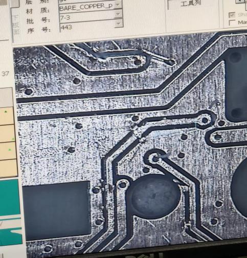
Other short-circuit findings were linked to physical scratching of board material or laminated dry film. Improving material handling and reducing damaging contact points were recommended. These observations underline a key principle: a defect appearing after dry film processing does not automatically mean the dry film caused it.
7. Production Verification Results
The darker HC-1538B material was evaluated across three LDI production groups. The report records 344 panels in total and the following AOI yields.
| Production Group | Quantity | Minimum Line Width / Spacing | AOI Yield |
|---|---|---|---|
| 420792 | 120 PNL | 0.225 / 0.10 mm | 90.13% |
| 220150 | 140 PNL | 0.125 / 0.12 mm | 92.5% |
| 220874 | 84 PNL | 0.15 / 0.12 mm | 91.27% |
The production follow-up concluded that the darker HC-1538B material showed production efficiency broadly consistent with the material already running on the line, and that its production and quality performance met the evaluated manufacturing requirements.
8. Practical Recommendations for PCB Manufacturers
- Do not reject dry film based only on visible color difference. Confirm actual imaging and production performance first.
- Confirm exposure energy regularly and use an exposure scale rather than visual judgment.
- When darker material shows slower image appearance, allow a suitable post-exposure holding time before deciding whether adjustment is needed.
- Verify exposure energy, developing point, and developing chemistry together.
- Investigate the whole PCB process. Plating contamination and physical scratches can be mistaken for dry film-related defects.
- Use AOI and batch-production data as the strongest basis for evaluating material performance.
Conclusion
Visible dry film color variation should be investigated, but color difference alone does not necessarily indicate a functional quality problem. In this HC-1538B evaluation, performance was assessed across surface preparation, lamination, LDI exposure, development, pattern plating, etching, and AOI inspection.
Stable PCB imaging depends on coordinated control of surface preparation, lamination, exposure, development, plating, etching, and inspection. A process-based evaluation helps distinguish material-related issues from process-related defects and reduces unnecessary production adjustments.
Technical Support
Guangdong Taiyada Optoelectronics Co., Ltd. supplies dry film photoresist for PCB manufacturing and provides technical support according to PCB structures, equipment, and production processes.
Website: taiyadafilm.com
Email: dryfilmtech@gmail.com