
Introduction
Dry film is used through several important stages of PCB circuit fabrication.
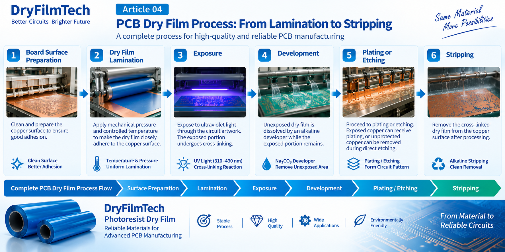
1. Board Surface Preparation
The copper surface is prepared to provide a clean and suitable surface for dry film adhesion.
2. Dry Film Lamination
Mechanical pressure and controlled temperature are used to make the dry film closely adhere to the copper surface.
3. Exposure
The dry film is exposed to ultraviolet light through the circuit artwork. The exposed portion undergoes cross-linking.
4. Development
The unexposed dry film is dissolved by an alkaline developer while the exposed portion remains.
5. Plating or Etching
Depending on the process, the developed board proceeds to plating or etching. Exposed copper can receive plating, or unprotected copper can be removed during direct etching.
6. Stripping
After processing, the cross-linked dry film is stripped from the copper surface.
Complete Process Flow
Surface Preparation → Lamination → Exposure → Development → Plating/Etching → Stripping
Conclusion
PCB dry film processing is a connected system. Stable conditions at every stage are important for consistent circuit quality.